Curriculum vitæ
Bibliometrics
h-index: 42 i10-index: 72 Citations: 11,406
Academic Career
2026 – present
Senior Staff Scientist in Electron Ptychography, The Rosalind Franklin Institute, Didcot, UK
2025 – 2026
PIFI Visiting Professor, University of the Chinese Academy of Sciences, Beijing, China
2019 – 2024
Assistant Professor, University of Antwerp, Belgium
ERC Principal Investigator of the project High Definition Electron
Microscopy
2017 – 2019
Scientist, Max-Planck-Institute for Solid State Research, Stuttgart,
Germany
2015 – 2017
Marie Skłodowska-Curie Fellow, Faculty of Physics, University of
Vienna, Austria
2014 – 2015
Postdoctoral Scientist, Faculty of Physics, University of Vienna, Austria
2012 – 2014
Staff Scientist, SuperSTEM Laboratory, UK
Postdoctoral Scientist, Department of Materials, University of
Oxford, UK
Education
2006 – 2012
Ph.D. in physics
Vanderbilt University and Oak Ridge National
Laboratory, USA
Understanding Materials through Scanning Transmission Electron
Microscopy & Density Functional Theory
Advisor: Prof. Sokrates T. Pantelides
2002 – 2006
B.A. in physics
Reed College, USA
Thesis: Three-state L-configuration electromagnetically induced transparency
Advisor: Prof. Danielle A. Braje
2004 – 2005
Undergraduate Research Internships at ORNL
The Scanning Transmission Electron Microscopy
Group, Oak Ridge National Laboratory, USA
Probing the spatial resolution of electron energy loss spectroscopy in complex oxides
Advisor: Dr. Maria Varela
Grants
Over €2.5M of funding obtained:
2022
Universiteit Antwerpen Bijzonder Onderzoeksfonds (210,000 Euros)
2021
Fonds Wetenschappelijk Onderzoek Fundamental Research Project
(461,000 Euros)
2020
Universiteit Antwerpen Bijzonder Onderzoeksfonds (210,000 Euros)
2019
ERC Starting grant (1,500,000 Euros)
2015
EC Marie Skłodowska-Curie Fellowship (166,157 Euros)
Teaching
2020 – 2024
Advanced Electron Microscopy Masters’ course in electron microscopy
Projects in Microscopy and Spectroscopy Masters’ research projects in electron microscopy and spectroscopy
2023 – 2024
Microscopy and spectroscopy of nanosystems Masters’ course in electron microscopy
Awards
2018
The Albert Crewe Award, Major award of the Microscopy Society of
America, their
highest for early career scientists working in the physical sciences.
Press release.
2015
European Microscopy Society Outstanding Paper Award in the Materials
Sciences category for Imaging screw dislocations at atomic resolution
by aberration-corrected electron optical sectioning, Nature
Communications 6, 7266 (2015)
2014
Birks Award for Best Contributed Paper from Microscopy & Microanalysis
2013 for Depth Sensitive Atomic Resolution Spectroscopy and Imaging
of Highly Strained YSZ/STO
Microscopy & Microanalysis Postdoctoral Award for Optical Sectioning with Atomic Resolution Spectroscopy
Second Place, 2014 Microscience and Microscopy Congress Poster Competition for Maximum efficiency phase contrast imaging in scanning transmission electron microscopy
2012
Best Oral Presentation, YUCOMAT conference for White Light Emission
from Fluctuating Nanoclusters
2010
International Federation of Societies for Microscopy Scholarship for
Strain-Enhanced Ionic Conductivity
Microscopy Society of America, Presidential Scholar Award for Strain-Enhanced Ionic Conductivity
2005
Microscopy and Microanalysis Graduate Student Poster Competition
Second Place, for Spatial Resolution of Spectroscopic Imaging in
Complex Oxides
Microscopy Society of America Undergraduate Research Scholarship for Atomic Scale Studies of Manganite Grain Boundaries with Colossal Magnetoresistance
Recognitions
2022
Applied Physics Letters
Editor’s Pick
C. Gao et al. “Overcoming contrast reversals in focused probe ptychography of thick materials: An optimal pipeline for efficiently determining local atomic structure in materials science”.
Applied Physics Letters, 121, 081906 (2022).
2017
Nature Nanotechnology Research
Highlight
R. Mirzayev et al. “Buckyball
sandwiches”.
Science Advances 3, e1700176 (2017).
2014
APS Physics Featured in
Physics
& IEEE Spectrum News
Release
C. Li et al. “Grain-Boundary-Enhanced Carrier Collection in CdTe
Solar Cells”. Physical
Review Letters 112, 15 (2014).
Nature Materials News &
Views
K. R. Paton et al. “Scalable production of large quantities of
defect-free few-layer graphene by shear exfoliation in
liquids”. Nature Materials 13,
(2014), p. 624.
Peer Review
Nature (Nature Group)
Nature Communications (Nature Group)
Scicence Advances (American Association for the Advancement of Science)
Ultramicroscopy (Elsevier)
PNAS (National Academy of Sciences)
Physical Review Letters (American Physical Society)
Physical Review X (American Physical Society)
Physical Review Research (American Physical Society)
Physical Review Applied (American Physical Society)
Chinese Physics B (IOP Publishing)
Nanoletters (American Chemical Society Publications)
Advanced Materials (Wiley)
Microscopy and Microanalysis (Cambridge University Press)
Microscopy (Oxford University Press)
Journal of Microscopy (The Royal Microscopical Society)\
Journal Covers
Selected Publications
-
B. Yuan, Z. Wang, S. Zhang, C. Hofer, C. Gao, T. Chennit, H. Shi, X. Wu, Y. Han, L. Dou, Y.Yu and T. J. Pennycook. “Atomically Resolved Edges and Defects in Lead Halide Perovskites”. Nature 687, 364 (2025).
Citations: 20
The lowest dose atomic resolution ptychography to date reveals the edge structure and dynamics of an organic hybrid perovskite for the first time, linking stability with the concentration and type of vacancies present. -
T. A. Bui, D. Lamprecht, J. Madsen, M. Kurpas, P. Kotrusz, A. Markevich, C. Mangler, J. Kotakoski, L. Filipovic, J. C. Meyer, T. J. Pennycook, V. Skákalová, K. Mustonen. “Hexatic phase in covalent two-dimensional silver iodide”. Science, 390, 1033 (2025).
Citations: 4
Time and temperature resolved STEM reveals the hexatic phase in a covalently bonded material, and provides evidence for the existence of a mixed melting scenario in 2D materials. -
R. Wang, Q. Zhao, L. Loetgering, F. Allars, Z. Hong, T. J. Pennycook, R. Horstmeyer, J. Rodenburg, A. Maiden and G. Zheng “Ptychography at all wavelengths ”. Nature Reviews Methods Primers, 5 (2025), p. 68.
Citations: 17
A review of ptychography as used across the disciplines, spanning a range of wavelengths from electrons (picometers) to visible light (micrometres). -
C. Hofer, J. Madsen, T. Susi and T. J. Pennycook. “Detecting charge transfer at defects in 2D materials with electron ptychography”. Journal of Microscopy, Ptychography Special Edition (2025), p. 1.
Citations: 15
Experimental demonstration of the sensitivity of ptychography to charge transfer due to bonding, including at defects. -
C. Hofer and T. J. Pennycook. “Reliable phase quantification in focused probe electron ptychography of thin materials”. Ultramicroscopy, 254 (2023), p. 113829.
Citations: 14
Introducing a superior method of quantifying the true atomic phases in ptychography and CoM based imaging. -
C. Gao, C. Hofer, D. Jannis, A. Béché, J. Verbeeck, and T. J. Pennycook. “Overcoming contrast reversals in focused probe ptychography of thick materials: An optimal pipeline for efficiently determining local atomic structure in materials science”. Applied Physics Letters, 121 (2022), p. 081906.
Citations: 25
Simultaneous ptychography complementing the Z-contrast workflow with no loss of speed, revealing light atoms and providing significantly greater dose efficiency than other STEM methods, including iCoM. -
H. S. Wang, L. Chen, K. Elibol, L. He, H. Wang, C. Chen, C. Jiang, C. Li, T. Wu, C. X. Cong, T. J. Pennycook, G. Argentero, D. Zhang, K. Watanabe, T. Taniguchi, W. Wei, Q. Yuan, J. C. Meyer and X. Xie. “Towards Chirality Control of Graphene Nanoribbons Embedded in Hexagonal Boron Nitride”. Nature Materials 20 (2021), p. 202.
Citations: 150
Edge-specific fabrication of graphene nanoribbons embedded in h-BN. -
D. Jannis, C. Hofer, C. Gao, X. Xie, A. Béché, T. J. Pennycook and J. Verbeeck. “Event Driven 4D STEM Acquisition With a Timepix3 Detector: Microsecond Dwell Time and Faster Scans for High Precision and Low Dose applications”. Ultramicroscopy 233 (2021), p. 113423.
Citations: 112
First 4D STEM unhindered by the speed of the camera. -
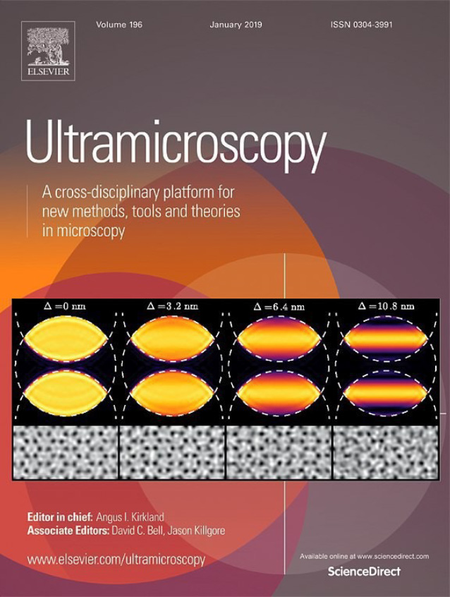
T. J. Pennycook, G. T. Martinez, P. D. Nellist, J. C. Meyer “High Dose Efficiency Atomic Resolution Imaging via Electron Ptychography”. Ultramicroscopy 196 (2019), p. 131.
Citations: 93
Superior low dose performance over conventional HRTEM with ptychography. -
T. J. Pennycook, H. Yang, L. Jones, A. R. Lupini, M. F. Murfitt and P. D. Nellist, “Efficient Phase Contrast Imaging in STEM Using a Pixelated Detector. Part 1: Experimental Demonstration at Atomic Resolution”. Ultramicroscopy 151, (2015), p. 160.
Citations: 343
Direct ptychography method for maximum efficiency imaging in STEM. -
K. R. Paton, E. Varrla, C. Backes, R. J. Smith, U. Khan, A. O’Neill, C. Boland, M. Lotya, O. M. Istrate, P. King, T. Higgins, S. Barwich, P. May, P. Puczkarski, I. Ahmed, M. Moebius, H. Pettersson, E. Long, J. Coelho, S. E. O’Brien, E. K. McGuire, B. M. Sanchez, G. S. Duesberg, N. McEvoy, T. J. Pennycook, C. Downing, A. Crossley, V. Nicolosi and J. N. Coleman. “Scalable Production of Large Quantities of Defect-Free Few-Layer Graphene by Shear Exfoliation in Liquids”. Nature Materials 13, (2014), p. 624.
Citations: 3041
Simple scalable production of large amounts of graphene. -
C. Li, Y. Wu, J. Poplawsky, T. J. Pennycook, N. Paudel, W. Yin, S. J. Haigh, M. P. Oxley, A. R. Lupini, M. Al-Jassim, S. J. Pennycook and Y. Yan. “Grain-Boundary-Enhanced Carrier Collection in CdTe Solar Cells”. Physical Review Letters 112 (2014), p. 156103.
Citations: 358
Physics behind the efficiency of CdTe solar cells. -
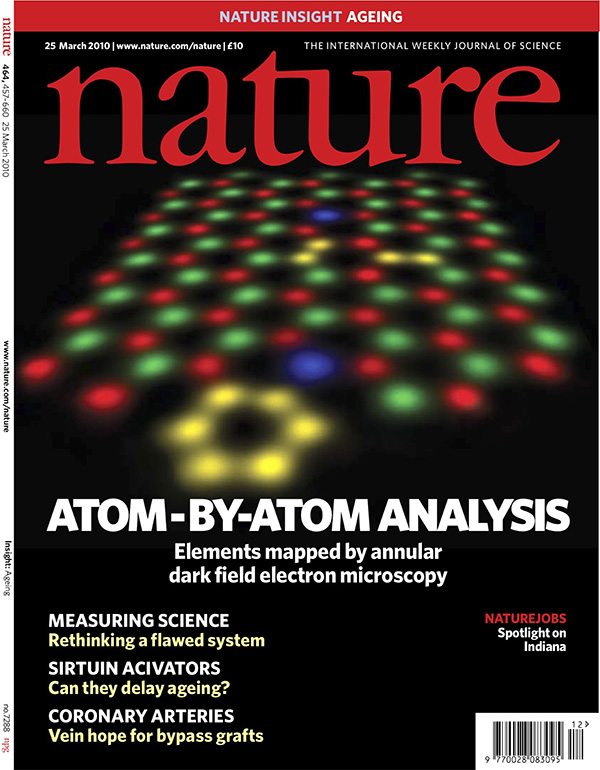
O. L. Krivanek, M. F. Chisholm, V. Nicolosi, T. J. Pennycook, G. J. Corbin, N. Dellby, M. F. Murfitt, C. S. Own, Z. S. Szilagyi, M. P. Oxley, S. T. Pantelides and S. J. Pennycook. “Atom-by-Atom Structural and Chemical Analysis by Annular Dark-Field Electron Microscopy”. Nature 464 (2010), p. 571.
Citations: 1676
Locating and identifying individual atoms in 2D materials.
Invited talks
2026
- Peking University, School of Materials Science and Engineering, Frontiers In Materials Science & Engineering Lecture (Beijing, China): “Electron Ptychography”
- University of Chinese Academy of Sciences, School of Physical Sciences Seminar, (Beijing, China): “Electron ptychography for highly beam sensitive materials and charge transfer detection”
- IAMNano 2025, (Gothenburg, Sweden): “Pushing Detection Limits with Electron Ptychography”
- Brookhaven National Lab, Center for Functional Nanomaterials, Research Seminar (Brookhaven, United States): “Electron ptychography with truly fast 4D STEM”
- NordTEMhub Workshop on 4D-STEM big data analysis (Trondheim, Norway): “Electron ptychography” talk and hands on session
- Ernst Ruska-Centre Seminar (Julich, Germany) "Electron ptychography and truly fast 4D STEM"
- Chinese Microscopy Society Meeting (Dongguan, China): "Electron ptychography and truly fast 4D STEM for deeper understanding of materials"
- SUSTech Physics Department Seminar (Shenzhen, China): "Fast 4D STEM and focused probe electron ptychography in STEM"
- ASML Research Seminar (Eindhoven, The Netherlands): "At the cutting edge in scanning transmission electron microscopy: 4D STEM and ptychography"
- University of Vienna, The Physics of Nanostructured Materials Seminar (Vienna, Austria): "The future of microscopy: 4D STEM and ptychography"
- NanED School on TEM Imaging and Spectroscopy (Antwerp, Belgium): "4D STEM and Ptychography"
- AdSTEM European School on 4D STEM Imaging (Piran, Slovenia): "An overview of 4D STEM and ptychography"
- AdSTEM European School on 4D STEM Imaging (Piran, Slovenia): "Making the most of 4D STEM with ptychography for applications ranging from ultralow dose to high precision studies"
- ASTAR Future of Microscopy Seminar (Singapore): "Seeing materials more clearly with 4D STEM and ptychography"
- Materials Research Society Fall Meeting (Boston, United States): "Fast and focused 4D STEM: an optimal pipeline for atomic resolution imaging in materials science"
- Faculty of Science Research Day, University of Antwerp (Antwerp, Belgium): "Seeing how atoms build materials"
- Frontiers of Electron Microscopy in Materials Science (FEMMS 2019) Conference: "From dynamics to high dose efficiency imaging in STEM"
- Microscopy & Microanalysis (M&M 2019) Conference: "Efficient phase contrast imaging via electron ptychography, a tutorial
- Royal Belgian Society for Microscopy (RBSM) Meeting: "Highly efficient phase contrast imaging in STEM with electron ptychography"
- EMAT Summer School on TEM, University of Antwerp: "Electron ptychography"
- University of Vienna Department of Physics Seminar: "Highly efficient phase contrast imaging in STEM with electron ptychography"
- 3rd Sino-German Symposium on Advanced Electron Microscopy and Spectroscopy, Beijing: "High-definition electron microscopy: Greater clarity via multidimensionality"
- EMAT Seminar, Department of Physics, University of Antwerp: "Achieving enhanced definition electron microscopy via quantitative phase imaging with ptychography"
- Directors' Board Meeting Lecture, Max Planck Institute of Solid State Research: "High-definition electron microscopy: Greater clarity via multidimensionality"
- Institute of Physics Seminar, Chinese Academy of Sciences, Beijing: "Seeing clearer: advancing transmission electron microscopy through multidimensional approaches from ptychography to optical sectioning"
- School of Physics Seminar, Peking University: "Advancing transmission electron microscopy through multidimensional approaches from ptychography to optical sectioning"
- International Ringberg Castle Workshop on Multidimensionality in Electron Microscopy: "Ptychography: Dose efficiency, aberration correction, and optical sectioning"
- StEM Seminar, Max Planck Institute of Solid State Research: "Phase contrast imaging of radiation sensitive materials using ptychography in a STEM"
- University of Vienna Department of Physics Seminar: "Phase contrast imaging of radiation sensitive materials using ptychography in a STEM'
- National University of Singapore Seminar: "Probing materials on the nanoscale with aberration-corrected STEM and first-principles theory"
- Max Planck Institute of Microstructure Physics Seminar, Halle: "Probing materials on the nanoscale with aberration-corrected STEM and first-principles theory"
- Department of Biology and Chemistry Seminar, Paul Scherrer Institute: "Ptychography in scanning transmission electron microscopy"
- Wuhan National Laboratory for Optoelectronics Seminar, Huazhong University of Science and Technology: "Probing atomic scale dynamics with Z-contrast STEM"
- Wuhan University Department of Physics Seminar: "Probing atomic scale dynamics with Z-contrast STEM"
- Physics of Nanostructured Materials Seminar, University of Vienna: "Frontiers in aberration corrected STEM "
- Nanoscale Physics Research Lab Seminar, School of Physics and Astronomy, The University of Birmingham: "Probing materials’ functionality on the nanoscale with aberration-corrected STEM and first-principles theory"
- European Materials Research Society (E-MRS) Fall Meeting: "Resolving the origin of materials’ properties with aberration-corrected STEM and first-principles theory"